

NVIDIA Optical Interconnect Investment, $4 B for Lumentum & Coherent, and 1.6 T AI Module Demand (2021 to 2026)
Optical Interconnect Projects, NVIDIA $4 B Investment, and 1.6 T Module Adoption
The industry has shifted from identifying the optical interconnect bottleneck before 2025 to pursuing aggressive, large-scale commercial deployments and strategic investments to resolve it, driven by the unsustainable power and data demands of artificial intelligence. Prior to 2024, the focus was on initial upgrades from copper to 400 G optical modules. The period from 2025 to 2026 marks a significant acceleration, characterized by mass deployments of 800 G and the rapid commercialization of 1.6 Terabit (1.6 T) technologies to prevent AI compute clusters from becoming data-starved.
- The adoption cycle has accelerated dramatically, with 800 G optical modules from companies like Ascent Optics achieving volume delivery in early 2026, while development of 1.6 T solutions by firms including POET Technologies and Lessengers moved toward sampling in Q 2 2026.
- This technology shift is driven by a power consumption crisis, as the energy required for data movement becomes a primary operational cost. A RAND Corporation forecast projected AI data center power needs to hit 68 GW by 2027, while Goldman Sachs projects a 160% increase in data center power demand by 2030, making the efficiency of optical interconnects a critical economic lever.
- The urgency is confirmed by financial commitments, with global data center capital expenditure surging 53% year-over-year in Q 1 2025. This includes direct strategic investments, such as NVIDIA‘s multi-billion dollar funding in optical component suppliers to secure its own GPU cluster supply chain.
- Hyperscalers like Meta, Google, and Amazon are driving this adoption, as the performance of their massive AI models is now limited more by data transfer speeds between GPUs than by the processing power of the chips themselves.
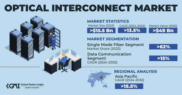
Optical Interconnect Market Forecasts Strong Growth
This chart provides the overall market growth context that justifies the significant NVIDIA investments and accelerated adoption of technologies like 1.6 T modules discussed in the section.
(Source: Global Market Insights)
$500 M Ayar Labs Funding and NVIDIA’s Optical Interconnect Investments
Corporate and venture capital investment in the optical interconnect sector intensified between 2025 and 2026, shifting from validating broad concepts to funding specific, scalable solutions like Co-Packaged Optics (CPO) and next-generation transceivers capable of meeting immediate AI infrastructure demands. This financial mobilization indicates market conviction that solving the interconnect bottleneck is a primary enabler for future AI growth.
- Venture funding targeted next-generation architectures, highlighted by Ayar Labs, a pioneer in CPO, securing a $500 million Series E round in March 2026 at a $3.75 billion valuation. This followed significant funding for other innovators, including Scintil Photonics ($58 million) and Teramount ($50 million).
- Strategic corporate investments became a key tool for securing supply chains, exemplified by NVIDIA‘s commitment of over $4 billion to key optical component suppliers Lumentum and Coherent. This move signals that leading AI chipmakers view the optical supply chain as a critical and vulnerable part of their ecosystem.
- Industry-wide collaboration materialized through consortium funding, with chiplet interconnect developer Eliyan raising $50 million in April 2026 from a group that included AMD, Arm, Intel Capital, and Meta. This signals a collective effort to standardize the crucial technology for in-package connectivity.
- The market’s high stakes were underscored by its volatility. On June 1, 2026, Celestial AI canceled all outstanding purchase orders for POET Technologies’ optical modules, demonstrating the significant commercial risks for suppliers in this rapidly evolving and competitive field.
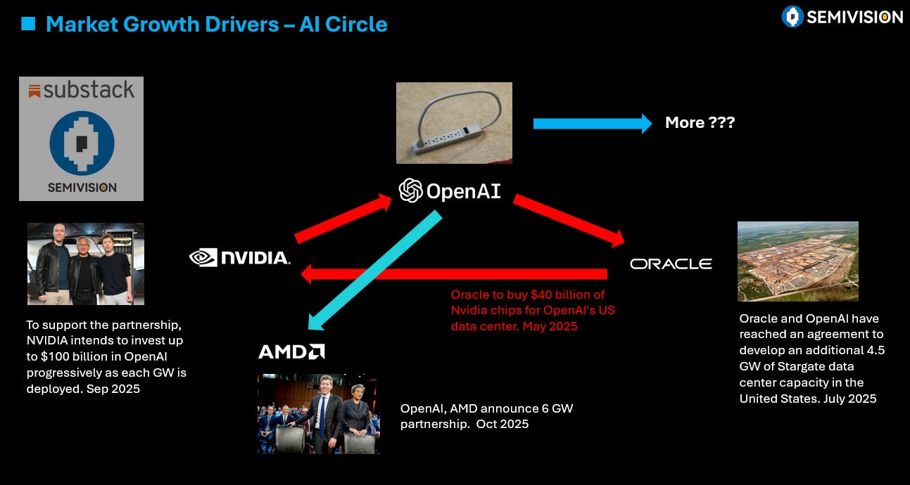
Massive AI Investments Drive Data Center Boom
The chart illustrates the macro-level investment boom in AI, which serves as the fundamental driver for the specific funding events, such as the Ayar Labs investment by NVIDIA, detailed in this section.
(Source: semivision – Substack)
Table: Strategic Investments in Optical Interconnect Technology (2025-2026)
| Company | Time Frame | Details and Strategic Purpose | Source |
|---|---|---|---|
| Ayar Labs | Mar 2026 | Raised $500 million in a Series E funding round at a $3.75 billion valuation. Funding is aimed at scaling production of its co-packaged optics solutions to meet demand from AI and high-performance computing customers. | Superb Crew |
| Avicena Tech | Apr 2026 | Raised $65 million in a Series B round. The company develops high-bandwidth, low-power optical interconnects based on micro LED technology, targeting chip-to-chip communication in AI systems. | Startup Intros |
| Eliyan | Apr 2026 | Raised $50 million from a strategic consortium including AMD, Arm, and Meta. The investment validates its chiplet interconnect technology, which enables high-speed, low-power communication between chiplets in a package. | Semiconductor Engineering |
| Xscape Photonics | Mar 2026 | Raised $37 million in new funding to support its laser-based optical interconnects. The technology aims to improve energy efficiency and bandwidth density for connections between chips and systems. | Silicon ANGLE |
| Scintil Photonics | Sep 2025 | Raised $58 million to scale its integrated photonics technology. The company focuses on augmented silicon photonic integrated circuits that integrate lasers, targeting 800 G and 1.6 T optical transceivers for AI data centers. | Scintil Photonics |
| Teramount | Nov 2025 | Raised $50 million in a Series A round led by Koch Disruptive Technologies. The funding is to scale its technology for connecting optical fibers to silicon chips, a critical step for high-volume manufacturing of co-packaged optics. | Koch Disruptive Technologies |
NVIDIA Optical Interconnect Partnerships for 1.6 T and Co-Packaged Optics
Strategic partnerships formed in 2025 and 2026 centered on accelerating the manufacturing and standardization of next-generation optical technologies, primarily 1.6 T modules and Co-Packaged Optics. Unlike earlier collaborations focused on research, these recent alliances are tactical, aiming to resolve immediate production and integration challenges to meet the aggressive timelines set by hyperscale AI infrastructure builders.
- Partnerships are targeting the accelerated development of next-generation modules. POET Technologies and Lumilens are collaborating on wafer-level photonic integration, while POET is separately working with Lessengers to co-develop 1.6 T optical modules, with samples anticipated in 2026.
- Major manufacturers are partnering directly with customers to scale production. STMicroelectronics announced it is quadrupling its 300 mm silicon photonics production capacity by 2027, a move explicitly aimed at meeting demand from its hyperscaler partners for high-volume, cost-effective components.
- The industry is moving toward standardization to create a stable ecosystem. In May 2026, a new industry coalition was launched to accelerate the deployment and create common standards for high-performance optical interconnects, recognizing that interoperability is essential for large-scale adoption.
- Foundries are partnering with startups on novel architectures. Nanosecond optical circuit switch developer Oriole began a collaboration with specialty foundry Tower Semiconductor to commercialize its technology, offering an alternative approach to traditional packet switching for specific AI workloads.
US vs. Asia, NVIDIA’s Optical Interconnect Supply Chain Focus
While North America maintains its lead in optical interconnect deployment and investment due to the heavy concentration of hyperscalers and AI companies, the period from 2025 to 2026 has been defined by a strategic restructuring of the manufacturing supply chain. Geopolitical tensions and government industrial policies are compelling a geographic diversification of production, primarily towards Southeast Asia, to mitigate risks and build sovereign capabilities.
- North America remains the largest market, accounting for 35% of demand according to Data M Intelligence, driven by the immense capital expenditures of US-based AI leaders. However, much of the manufacturing remains offshore. The grid infrastructure needed to support these data centers, especially in regions like Virginia, is also a growing concern.
- Asia-Pacific is both a major growth market (30% share) and a critical manufacturing hub. In response to geopolitical risks associated with China, US firms are actively expanding production of optical components in countries across Southeast Asia, as highlighted by Trend Force analysis in May 2026.
- Government incentives are directly shaping the geographic landscape. The U.S. CHIPS Act and the EU Chips Act provide billions in subsidies and investment tax credits of up to 25% to encourage domestic manufacturing. A direct outcome was the $20.9 million grant from the Texas Semiconductor Innovation Fund to Applied Optoelectronics in April 2026 to expand its Texas-based production.
- This restructuring is increasingly viewed through a lens of supply chain sovereignty. U.S. export controls on AI infrastructure and concerns over China’s control of critical materials like gallium have elevated advanced component manufacturing to a matter of strategic national security.
NVIDIA and the Shift From Pluggable Optics to Co-Packaged Solutions
The optical interconnect market is at a technology inflection point, transitioning from mature but power-intensive pluggable modules to the early commercialization of more integrated and efficient solutions like Co-Packaged Optics (CPO). While 800 G and 1.6 T pluggable modules represent the current commercial standard for scaling AI clusters, the industry recognizes that their power consumption and density limitations make them an intermediate solution. CPO is widely seen as the necessary next step for long-term scalability.
- Pluggable optical modules have reached mass deployment and are considered a mature technology. 800 G modules became widely available in 2025, and 1.6 T modules began volume shipments in April 2026. These components are essential for current AI build-outs but consume a significant portion of the network power budget.
- Co-Packaged Optics (CPO) is now an emerging commercial technology. After years in development, CPO is attracting major investment and is projected to constitute roughly 35% of AI data center optical modules by 2030. This technology moves the optical I/O directly onto the processor substrate, drastically reducing power consumption by shortening the electrical path.
- Silicon Photonics is the foundational enabling technology that has reached maturity. Its use of standard CMOS processes allows for the high-volume, cost-effective manufacturing of optical components, and major players like Intel and STMicroelectronics are heavily invested in expanding their production capacity.
- Alternative architectures like Optical Circuit Switching (OCS) remain at a niche or R&D stage. While companies like Oriole are working to commercialize the technology for ultra-low latency applications, it is not yet a mainstream solution for general-purpose AI interconnects.
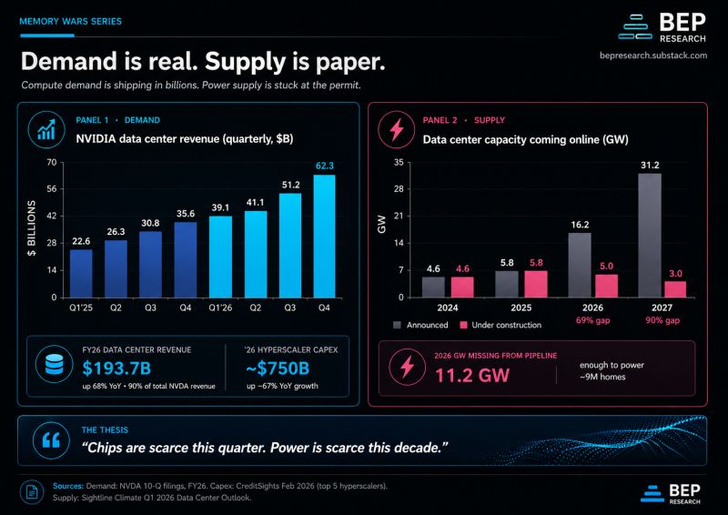
AI Compute Demand Outpaces Data Center Power Supply
The chart highlights the critical power supply challenge created by AI demand, which is the primary motivation for the technological shift from traditional pluggable optics to more power-efficient co-packaged solutions discussed in this section.
(Source: LinkedIn)
SWOT Analysis: NVIDIA and the Optical Interconnect Market
The optical interconnect market’s core strength lies in its indispensable role in enabling AI growth, attracting massive and non-discretionary capital from hyperscalers. However, this strength is offset by the significant weakness of high power consumption and manufacturing complexity in current-generation technologies. This tension creates substantial opportunities for disruptive, integrated solutions like Co-Packaged Optics while simultaneously exposing the entire AI hardware ecosystem to significant supply chain and geopolitical threats.
- The market’s trajectory is propelled by the undeniable demand from AI, but its primary threat is the increasing fragility and politicization of the global semiconductor supply chain.
- Opportunities are concentrated in technological advancements that address the core weakness of power inefficiency, with CPO and silicon photonics at the forefront.
- The primary strategic challenge is for companies to navigate the transition from profitable, mature pluggable modules to the next generation of integrated optics without succumbing to the high risks of a volatile and rapidly changing market.
Table: SWOT Analysis for the Optical Interconnect Market
| SWOT Category | 2021 – 2023 | 2024 – 2025 | What Changed / Validated |
|---|---|---|---|
| Strengths | Growing demand from data centers and telecom; established pluggable module ecosystem. | Exponential, non-discretionary demand from AI; massive CAPEX from hyperscalers ($320 B in 2025); clear performance advantages over copper. | The market validated that AI cannot scale without advanced optical interconnects, making it a critical, non-negotiable component of AI infrastructure. |
| Weaknesses | High cost per bit compared to copper at lower speeds; fragmented standards. | High power consumption and heat generation of 800 G/1.6 T pluggables (“power wall”); manufacturing complexity and cost of CPO. | The “power wall” became a primary economic and technical barrier, validating that simply increasing pluggable speed is not a sustainable long-term strategy. |
| Opportunities | Emergence of 400 G; initial research into co-packaged optics (CPO). | Massive investment in CPO (Ayar Labs’ $500 M round); government incentives (CHIPS Act); new architectures like Optical Circuit Switching (OCS). | The market validated CPO as the primary technological path forward, attracting immense strategic and venture capital to solve its integration and manufacturing challenges. |
| Threats | Supply chain disruptions from COVID-19; competition from advanced copper links. | Geopolitical supply chain risks (US/China, critical materials like gallium); high market volatility (e.g., Celestial AI/POET cancellation); thermal limits for future 3.2 T+ modules. | Geopolitical risk shifted from a theoretical concern to a primary driver of supply chain strategy, forcing geographic diversification and onshoring initiatives. |
NVIDIA 2026 Outlook: CPO Adoption and Interconnect Supply Chain Risk
The most critical strategic development to monitor over the next 12-18 months is the first confirmed large-scale deployment of Co-Packaged Optics (CPO) within a next-generation AI accelerator by a major hyperscaler or chip designer like NVIDIA. Such an event would serve as the ultimate validation of CPO’s commercial readiness, likely triggering a rapid realignment of the supply chain and investment landscape as the rest of the industry races to follow.
- If this happens: Watch for official product announcements or teardown analyses revealing CPO technology from pioneers like Ayar Labs integrated into new GPU, TPU, or custom ASIC designs from a major cloud provider. This would confirm that CPO has overcome the hurdles of yield, thermal management, and reliability at scale. The energy implications for these massive AI data centers would be significant.
- Then watch this: Following a successful CPO deployment, expect a surge in mergers and acquisitions as larger semiconductor and networking companies move to acquire CPO startups and related technology providers. Additionally, monitor for announcements from major semiconductor foundries establishing dedicated, high-volume manufacturing lines specifically for CPO integration.
- These could be happening: Conversely, if CPO deployment announcements are delayed into 2027, it would signal that significant technical or economic challenges remain. In this scenario, expect the industry to double down on the existing pluggable module roadmap, with an even more aggressive push for 1.6 T and early 3.2 T solutions. This would sustain the profitability of incumbent module makers but exacerbate long-term concerns around data center power consumption and physical density.
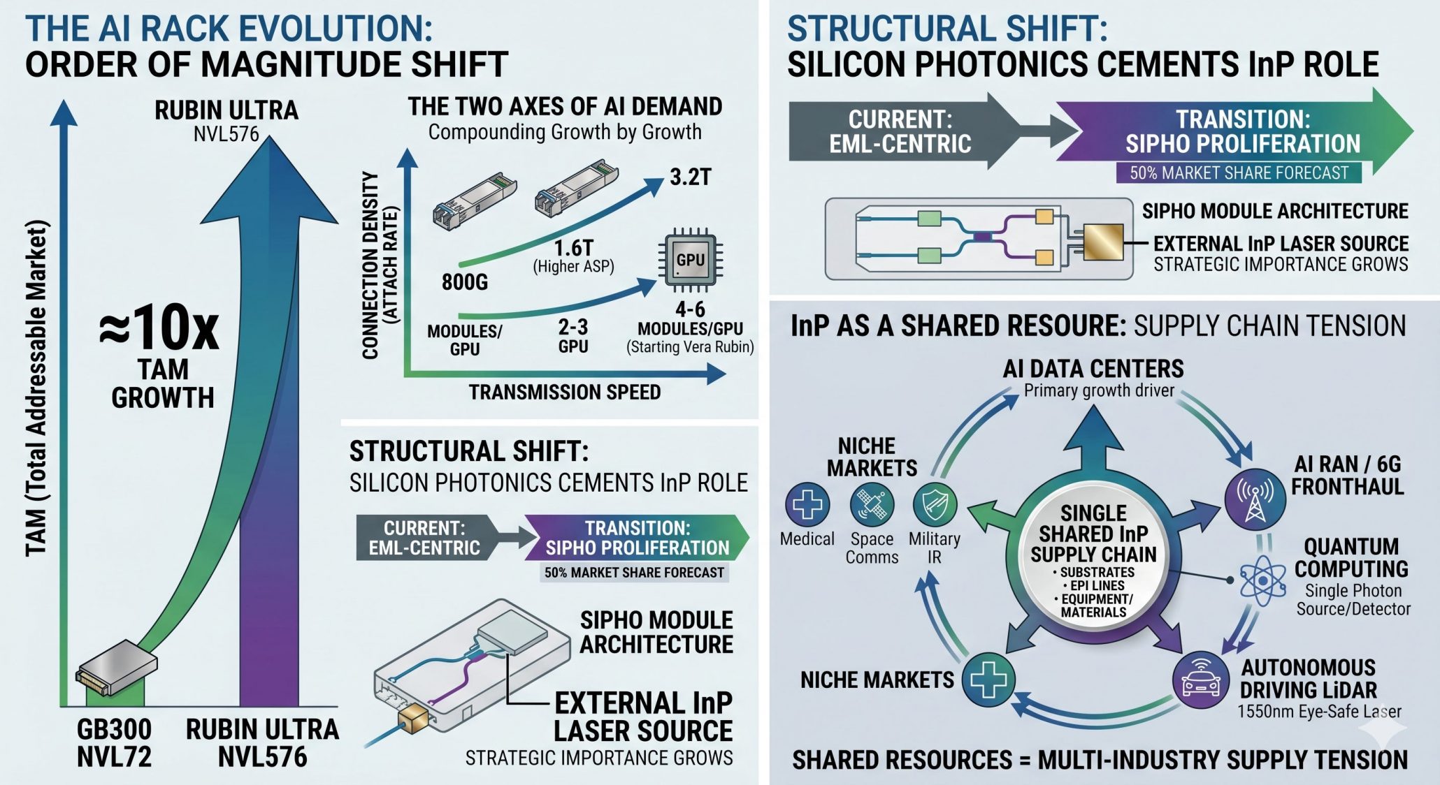
AI Drives Optical Shift, Creates InP Bottleneck
This chart provides a specific example of a “Supply Chain Risk”—the InP bottleneck—which is a key theme of the 2026 outlook discussed in this section.
(Source: Damnang’s Substack)
The questions your competitors are already asking
This report covers one angle of the commercial and strategic response to the AI optical interconnect gap. The questions that matter most depend on your work.
- Which companies are gaining or losing ground in the 800 G and 1.6 T optical interconnect market for AI?
- What is the outlook for 1.6 T optical module deployment in AI data centers by 2026?
- How does 1.6 T optical interconnect technology compare to 800 G for power efficiency and cost in large AI clusters?
- Who are NVIDIA’s key optical interconnect suppliers for its AI compute platforms?
This report does not answer these. Enki Brief Pro does.
Your question, your angle, your framework. SWOT, PESTL, scenario modelling. The same niche depth, built around the decision your work actually depends on.