

AI’s Power Wall: Why Advanced Memory and Packaging Dictate 2026 Infrastructure Costs and Grid Strain
Commercial Adoption of Advanced Memory Signals a Shift from Performance to Cost and Power Mitigation
The industry’s focus has decisively shifted from scaling raw compute power to mitigating the unsustainable energy and data movement costs of AI, driving the adoption of integrated memory and packaging solutions as a primary constraint management strategy. This transition reflects a market-wide recognition that the “memory wall” and “power wall” are no longer theoretical limits but immediate operational and financial burdens.
- Between 2021 and 2024, the adoption of technologies like High-Bandwidth Memory (HBM) and 2.5 D packaging was primarily driven by the pursuit of maximum performance for training large AI models. During this period, companies like Untether AI and En Charge AI were in earlier research phases, exploring at-memory compute architectures to address the underlying data movement problem for future applications.
- From 2025 to today, the narrative has pivoted from performance enhancement to crisis management. The entire 2026 supply of high-end AI memory is reportedly sold out, a situation created not just by demand for more FLOPs, but by an urgent need to manage the “power wall.” Projections showing future accelerators consuming up to 15, 000 watts have made energy efficiency the dominant driver for adopting new memory and packaging designs.
- This strategic shift is confirmed by the diversification of adopted solutions. While HBM remains essential for high-end training, new collaborations like the one between d-Matrix and Alchip on an inference-specific 3 D-stacked DRAM solution are emerging. This shows the market is segmenting to attack the power and cost problem from multiple angles, optimizing for different workloads beyond just training.
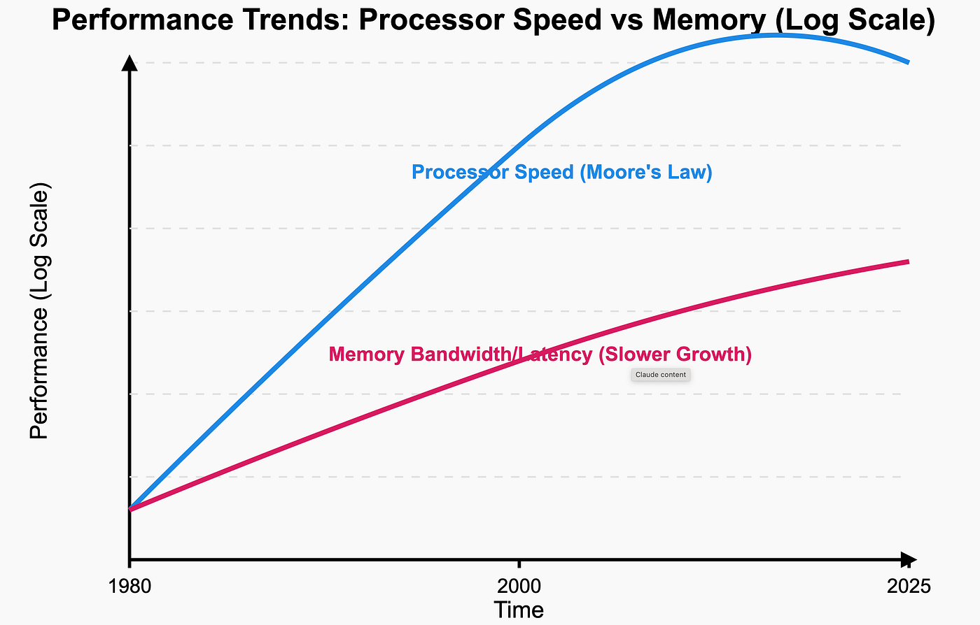
The ‘Memory Wall’ Drives Industry Shift
This chart illustrates the ‘memory wall,’ the widening performance gap between processors and memory, which is the core problem driving the industry’s strategic shift toward cost and power mitigation.
(Source: Medium)
Capital Expenditure Soars as Industry Invests to Overcome Memory and Packaging Bottlenecks
Unprecedented capital expenditures are being directed into the AI hardware ecosystem, with a clear strategic focus on securing the advanced memory and packaging capacity required to manage spiraling operational costs and future power demands. These investments are no longer just for building more data centers but for fundamentally re-architecting the hardware within them.

Hyperscaler Capex Fuels AI Chip Growth
This chart directly quantifies the section’s main point, showing how massive capital expenditure from hyperscalers is the primary driver for the growing AI chip market.
(Source: IDTechEx)
- Corporate AI capital expenditure is projected to exceed $500 billion in 2026 alone, a massive increase driven by hyperscalers like Microsoft making record investments in specialized AI hardware that heavily relies on advanced memory configurations. This spending reflects the high cost of overcoming data movement bottlenecks at scale.
- Memory manufacturers are making targeted, multi-billion-dollar investments to address the bottleneck directly. SK Hynix‘s commitment of nearly $4 billion for an advanced packaging facility in Indiana and over $1 billion in South Korea is not just for increasing memory volume but specifically for advancing the packaging technologies that integrate memory and logic more efficiently.
- Public funding is now also prioritizing energy efficiency, validating the private sector’s focus. The U.S. Department of Defense’s $16.3 million award to a Stanford and UC Berkeley-led AI hardware hub is aimed at creating “ultra-efficient” hardware, reinforcing that the national investment thesis is centered on improving performance-per-watt.
Table: Key Investments in AI Memory and Packaging Infrastructure
| Partner / Project | Time Frame | Details and Strategic Purpose | Source |
|---|---|---|---|
| SK Hynix / Purdue Research Park | 2024 | Investment of nearly $4 billion to establish an advanced packaging fabrication and R&D facility for AI memory chips. This move aims to build a U.S.-based supply chain for critical HBM components. | engineering.purdue.edu |
| Stanford & UC Berkeley / U.S. Do D | 2024 | Awarded $16.3 million to an AI hardware hub focused on developing ultra-efficient hardware. The goal is to address the power consumption constraints of next-generation AI systems. | engineering.berkeley.edu |
| SK Hynix / South Korea Facility | 2024 | Investment of over $1 billion to expand and improve the final steps of chip manufacturing, focusing on critical HBM packaging technologies like MR-MUF and TSV to maintain its market lead. | financialpost.com |
| Goldman Sachs Forecast | 2025 | Projected that global corporate capital expenditures on AI infrastructure could exceed $500 billion in 2026, driven by the massive hardware requirements for data center buildouts. | goldmansachs.com |
Strategic Co-Design Partnerships Target AI’s Core Power and Data Bottlenecks
Strategic alliances in the semiconductor industry have evolved from simple supplier-customer relationships to deep, co-design partnerships. These collaborations are aimed at solving the fundamental physics of data movement and power consumption in AI systems, signaling that integrated system design is now the primary path to future scaling.

Future Chips Integrate Memory and Compute
This diagram of a future System-in-Package perfectly visualizes the outcome of the ‘co-design partnerships’ and ‘integrated system design’ described in the section.
(Source: semivision – Substack)
- Before 2025, partnerships were often focused on integrating existing technologies or exploring novel concepts in an R&D context. The research partnership between startup Tetra Mem and memory giant SK Hynix to investigate in-memory computing is a key example of this earlier, more exploratory phase.
- The period from 2025 to today is defined by the formation of long-term alliances to create new technology standards. The landmark collaboration between Intel and Soft Bank subsidiary SAIMEMORY to develop Z-Angle Memory (ZAM), with a commercialization target of 2029, represents a new class of partnership aimed at fundamentally redesigning memory for power efficiency.
- This trend extends across the supply chain, with equipment manufacturers like Applied Materials establishing new collaboration models with chipmakers. These initiatives aim to accelerate R&D in advanced packaging, acknowledging that no single company can solve the tightly coupled challenges of memory, logic, and integration alone.
Table: Notable Alliances in AI Memory and Packaging
| Partner / Project | Time Frame | Details and Strategic Purpose | Source |
|---|---|---|---|
| Intel & SAIMEMORY (Soft Bank) | 2026 | A long-term collaboration to develop Z-Angle Memory (ZAM), a new DRAM-based architecture. The explicit goals are to address the memory performance and power consumption bottlenecks of AI, with commercialization targeted for 2029. | insidehpc.com |
| d-Matrix & Alchip | 2025 | Announced a collaboration on what they claim will be the world’s first 3 D-stacked DRAM solution specifically for AI inference. The goal is to deliver up to 10 times faster inference performance than systems based on the forthcoming HBM 4 standard. | alchip.com |
| Applied Materials / Singapore R&D Hub | 2024 | Launched a new collaboration model to bring together top semiconductor R&D leaders in Singapore. The initiative is designed to accelerate innovation in high-performance, low-power AI chip packaging technologies. | ir.appliedmaterials.com |
| Tetra Mem Inc. & SK hynix | 2024 | Signed a Statement of Work for a joint research project on in-memory computing technologies. This partnership connects an innovative startup with a leading memory manufacturer to explore post-Von Neumann architectures. | prnewswire.com |
Geographic Investment in Advanced Packaging Shifts to Mitigate Supply Chain Risk
The geographic distribution of advanced memory and packaging investment is concentrating in regions that can support the entire high-value manufacturing ecosystem. This represents a strategic shift from a historical focus on pure fabrication in Asia to the development of integrated packaging and R&D hubs in the United States and other regions to ensure supply chain resilience.
- Between 2021 and 2024, the AI hardware supply chain was heavily concentrated in Asia, with South Korea (SK Hynix, Samsung) and Taiwan (TSMC) dominating HBM manufacturing and advanced foundry services, respectively. Packaging was often seen as a final, lower-value step in this process.
- Starting in 2024 and accelerating into 2025, a clear trend of onshoring critical packaging capabilities to the U.S. emerged. SK Hynix‘s decision to invest nearly $4 billion in an Indiana advanced packaging facility is the most significant example, directly linking high-volume manufacturing with a U.S. R&D ecosystem at Purdue University.
- This reshoring is driven by strategic imperatives beyond logistics. The formation of a Silicon Valley consortium to advance 2.5 D and 3 D packaging R&D underscores a U.S. national strategy to build domestic expertise, based on the recognition that leadership in packaging is now inseparable from leadership in AI.
Technology Maturity: HBM Supply Crisis Accelerates Commercialization of Alternatives
While High-Bandwidth Memory and 2.5 D packaging are mature, commercially scaled technologies, the acute pressure from the power wall and supply constraints is accelerating the development and validation of next-generation solutions. Technologies that were once in R&D are now on clear paths to commercial adoption to address the limitations of the current standard.
- In the 2021-2024 period, the market was characterized by the generational evolution of HBM (HBM 2 E, HBM 3), which became the established standard for high-end AI accelerators. Competing technologies like in-memory computing and Compute Express Link (CXL) were largely in early research or specification development phases.
- From 2025 onward, the market dynamic changed. The global shortage of HBM, with supply for 2026 already sold out, has validated its status as an indispensable technology while simultaneously exposing its limitations in scalability and cost. This has created a strong commercial pull for alternatives.
- This pull is accelerating timelines for next-generation solutions. The d-Matrix and Alchip partnership is targeting a 2026-2027 launch for its inference-optimized 3 D-stacked DRAM. Meanwhile, CXL is moving from a paper standard to a deployed data center technology, with CXL 3.0+ enabling the memory pooling needed to manage massive AI models efficiently.
SWOT Analysis: Advanced Memory and Packaging as a Scaling Vector for AI
The strategic pivot to advanced memory and packaging has created significant opportunities for performance-per-watt gains, but it also introduces new weaknesses in supply chain concentration and exposes the industry to threats from unsustainable power demand and spiraling capital costs.
Table: SWOT Analysis for Advanced Memory and Packaging in AI
| SWOT Category | 2021 – 2024 | 2025 – Today | What Changed / Resolved / Validated |
|---|---|---|---|
| Strengths | Enabled significant performance gains in AI training via higher bandwidth (e.g., HBM 3). Heterogeneous integration allowed for optimization of different chiplets on different process nodes. | The primary strength has shifted to improving performance-per-watt, directly addressing the “power wall.” Architectures are now co-designed to minimize energy-intensive data movement. | The value proposition shifted from pure performance to a balance of performance, power efficiency, and operational cost, validating memory-centric design as a primary scaling vector. |
| Weaknesses | High cost and manufacturing complexity of 2.5 D interposers and HBM stacking. Dependence on a few key suppliers (TSMC, SK Hynix, Samsung) for critical components. | An acute global supply shortage of HBM has become a major production bottleneck for the entire AI industry. The extreme cost of HBM constrains hardware availability and drives up total system cost. | The weakness of supply chain concentration was validated by the HBM shortage in 2025-2026, which is now a primary constraint on AI hardware deployment. |
| Opportunities | The “More than Moore” paradigm created opportunities for startups in chiplet design and novel interconnects. CXL emerged as a standard for future memory disaggregation. | The limitations of HBM have created market opportunities for alternative architectures like Intel‘s ZAM and inference-specific 3 D DRAM (d-Matrix). Memory pooling via CXL is now a commercial reality. | The market validated the need for a diversified set of memory solutions beyond HBM, creating clear commercialization paths for technologies that were previously in R&D. |
| Threats | Increasing power consumption of AI accelerators was a growing concern. The complexity of heterogeneous integration posed significant design and verification challenges. | The “power wall” has become an existential threat, with projections of 15, 000 W accelerators. Massive capex cycles ($500 B+ in 2026) risk financial instability and strain on the electrical grid. | The threat of unsustainable power consumption was validated by concrete projections and the massive capital investments required, making it a central concern for investors and grid operators. |
2026 Scenario: Watch for a Break in the AI Power Consumption Curve
The single most critical indicator for the future of AI scaling is the industry’s ability to bend the projected power consumption curve through memory-centric efficiency gains, as the current trajectory is unsustainable both financially and environmentally.

GPU Complexity Growth Fuels Power Concerns
This chart’s depiction of skyrocketing GPU complexity and compute demand provides a direct visual for the ‘unsustainable power consumption curve’ that the section identifies as a critical issue.
(Source: SemiWiki)
- If this happens: If next-generation AI accelerators, such as NVIDIA’s upcoming Rubin platform and its successors, continue on the projected path toward 15, 000 watts per chip, the operational cost and infrastructure requirements will become prohibitive for all but a handful of hyperscalers.
- Watch this: Monitor the adoption rate and, more importantly, the performance-per-watt benchmarks of alternative architectures like Intel’s ZAM and d-Matrix’s 3 D-stacked DRAM. A significant uptick in their deployment by 2027-2029 would be a leading indicator that the industry is successfully diversifying its hardware base to manage power. Also, watch for any easing in the HBM supply chain, as this could signal a shift in demand toward these more efficient alternatives.
- These could be happening: A failure to commercialize these more efficient memory solutions on schedule will likely lead to a bifurcation of the AI market. One segment will be defined by extremely high-cost, power-hungry frontier models, while a larger segment will be forced to focus on smaller, less capable models that can run on existing infrastructure. This could slow the pace of broad AI innovation and deployment due to insurmountable power and cost barriers.
Frequently Asked Questions
Why is the AI industry suddenly so focused on memory and packaging instead of just making faster chips?
The industry’s focus has shifted because the energy and data movement costs of AI have become unsustainable. Simply making processors faster without addressing the ‘memory wall’—the bottleneck in moving data to the chip—leads to massive power consumption. Advanced memory (like HBM) and packaging technologies bring memory and logic closer together, reducing the energy wasted on data movement and directly addressing the ‘power wall’ as a primary strategy for cost and energy management.
What are the ‘power wall’ and ‘memory wall,’ and why are they a problem now?
The ‘memory wall’ is the bottleneck caused by the limited speed of moving data between memory and the processor. The ‘power wall’ is the practical limit where AI accelerators consume so much electricity (with projections of up to 15,000 watts per chip) that they become too expensive to cool and operate, placing an unsustainable strain on data center infrastructure and the electrical grid. These have become urgent problems now because the massive scale of modern AI models has turned these issues from theoretical limits into immediate financial and operational crises.
The article says High-Bandwidth Memory (HBM) is sold out for 2026. What are the alternatives being developed?
While HBM is the current standard for high-performance AI training, its supply constraints and high cost have spurred the development of alternatives. Key alternatives mentioned include: 1) Inference-specific 3D-stacked DRAM, like the solution from d-Matrix and Alchip, designed for better performance and power on inference tasks. 2) New memory architectures like Z-Angle Memory (ZAM), being developed by Intel and SAIMEMORY with a target for 2029 commercialization. 3) Technologies like Compute Express Link (CXL), which allows for ‘memory pooling’ to more efficiently manage memory resources across a data center.
Why is so much money (over $500 billion in 2026) being invested in AI hardware?
The massive capital expenditure isn’t just for building more data centers, but for fundamentally re-architecting the hardware within them to be more efficient. A large portion of this investment, such as SK Hynix’s nearly $4 billion facility in Indiana, is specifically targeted at advanced memory and packaging. This is a direct response to the ‘power wall,’ as companies are investing heavily to secure the next-generation hardware required to manage spiraling operational costs and future power demands.
What is the most critical indicator to watch to see if the industry can solve its power consumption problem?
The single most critical indicator is the performance-per-watt of next-generation AI hardware. Specifically, you should monitor the adoption rate and efficiency benchmarks of alternative memory architectures like Intel’s ZAM and d-Matrix’s 3D-stacked DRAM between 2027 and 2029. A significant increase in their deployment would show that the industry is successfully diversifying its hardware to manage power. Conversely, a failure to commercialize these solutions could lead to a future where only a few hyperscalers can afford to run frontier AI models.
Experience In-Depth, Real-Time Analysis
For just $200/year (not $200/hour). Stop wasting time with alternatives:
- Consultancies take weeks and cost thousands.
- ChatGPT and Perplexity lack depth.
- Googling wastes hours with scattered results.
Enki delivers fresh, evidence-based insights covering your market, your customers, and your competitors.
Trusted by Fortune 500 teams. Market-specific intelligence.
Explore Your Market →One-week free trial. Cancel anytime.